STUDY OF SPIN TRANSFER TORQUE (STT) AND SPIN ORBIT TORQUE (SOT) MAGNETIC TUNNEL JUNCTIONS (MTJS) AT ADVANCED CMOS TECHNOLOGY NODES
Jabeur, G. Di Pendina and G. Prenat
Univ. Grenoble Alpes, INAC-SPINTEC, F-38000 Grenoble, France; CNRS, INAC-SPINTEC, F-38000 Grenoble, France; and CEA, INAC-SPINTEC, F-38000 Grenoble, France
Abstract
Magnetic Random Access Memory (MRAM) is a promising candidate to be the universal non-volatile (NV) storage device. The Magnetic Tunnel Junction (MTJ) is the cornerstone of the NV-MRAM technology. 2-terminal MTJ based on Spin Transfer Torque (STT) switching is considered as a hot topic for academic and industrial researchers. Moreover, the 3-terminal Spin Orbit Torque (SOT) MTJ has recently been considered as a hopeful device which provides an increased reliability thanks to independent write and read paths. Since both MTJ devices (STT and SOT) seem to revolutionize the data storage market, it is necessary to explore their compatibility with very advanced CMOS processes in terms of transistor sizing and performance. Assuming a good maturity of the magnetic processes that would enable to fabricate small junctions, simulation results show that the existing advanced sub-micronic CMOS processes can drive the required writing current with reasonable size of transistors confirming the high density feature of MRAMs. At 28 nm node, the minimum transistor size can be used by the STT device. The SOT device shows remarkable energy efficiency with 6× improvement compared with the STT technology. Results are very encouraging for future complex hybrid magnetic/CMOS integrated circuits (ICs).
Keywords
MRAM, Magnetic Tunnel junction, Spin Hall Effect, Spin Orbit torque, Spin Transfer torque.
1.Introduction
The intensive research effort in spintronics invigorates the dream of IC designers to conceive a memory which gathers most merits encountered separately in existing random access memories (RAMs). In other words, a device which combines the high density of Dynamic RAMs (DRAMs), the rapidity and robustness of Static RAMs (SRAMs) and the non-volatility (NV) of Flash memories. In addition to all these latter assets, MRAMs based on MTJs offer high endurance and intrinsic hardness to radiation. Besides, the NV feature of MTJs makes them very attractive for Application Specific Integrated Circuits (ASICs) applications. For instance, NV flip-flops can be designed to be used as a primitive cell into the ASIC design library offering safety, power reduction and instant on/off [1]. By view of this fact, both memory and logic design communities are interested in the integration of MTJs with CMOS circuits.
The switching mechanisms of MTJ determine the power, speed and area performances of hybrid MTJ/CMOS circuits. The early generation of MTJs commercialized by Everspin, was based on Field Induced Magnetic Switching (FIMS) [2] writing scheme. A later improvement was proposed by Crocus by thermally assisting the writing operation (TAS) [3]. The high switching current of FIMS (>10mA) and TAS (>1mA) limits significantly their future use for memory application and bring the dynamic power issue for the logic circuits. A great interest is now given for the Spin-Transfer Torque (STT) switching approach which requires a lower current (e.g. <100 µA) to reverse the state of MTJ [4] [5]. The high scalability of STT-MTJs opens up new horizons for commercial applications of hybrid MTJ/CMOS circuits. However, the 2-terminal structure of the STT device exhibits a common write and read path. This hints two major shortcoming limiting the reliability of the device; i) the high current density required for writing can occasionally damage the MTJ barrier, ii) it remains a challenge to fulfill a reliable reading without ever causing switching. Recently, in 2011, the possibility of a fourth magnetization switching approach known as “Spin-Orbit-Torque” (SOT) has been proved [6]. Such a writing scheme uses an in-plane induced current to reverse the state of the MTJ without passing through the junction. The 3-terminal geometry of the SOT device separates the writing path from the reading path, thus the reliability issues encountered with the STT-MTJ are omitted.
Following the evolution of MTJ devices, current research is mainly focused on SOT and STT switching. It is expected that the potential of MTJ based circuits is enhanced at advanced nodes (below 65 nm). In this work, we study the compatibility of MTJs with advanced CMOS processes based on 65 nm, 40 nm and 28 nm. In the three cases, we used MOS transistors from Low Power (LP) and Standard Threshold-voltage (SVt) design kit library. The SOT and STT technologies are compared in terms of the required MOS transistor size and the writing energy per bit cell.
Section 2 describes both STT and SOT devices as well as their writing mechanism. In section 3, we evaluate the required transistor size per bit cell as well as the required energy to write the MTJ. Section 4 is the discussion
2.Description of STT and SOT devices
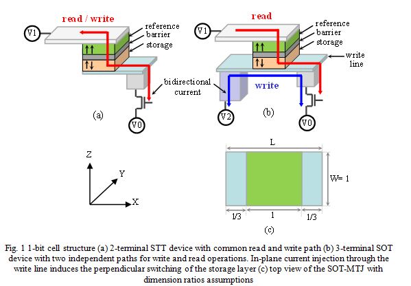
The basic structure of an MTJ device is composed of 2 Ferro-Magnetic (FM) layers separated by an insulator. Both layers have an intrinsic magnetization. The first FM layer (hard layer) -with a pinned magnetization- acts as a reference while the second FM layer (soft layer) -with a free magnetization- acts as a storage layer, (figure 1). The magnetization of the storage layer can be switched between two stable states, either parallel (P) or antiparallel (AP) with respect to the reference layer. Electrons can tunnel through the thin barrier (~1nm) when a bias voltage is applied between the two electrodes of the device. The MTJ resistance is low (or high) for a P (or AP) magnetization configuration. Devices based on Perpendicular magnetic anisotropy (PMA) materials have an improved thermal stability and scale better than in-plane magnetic anisotropy (IMA) material-based [4] [5]. Thus, both STT and SOT MTJs studied in this letter are PMA materials-based.
Figure 1 (a) shows the 2-terminal architecture of the STT-MTJ with the same read and write path. Figure 1(b) shows the SOT-MTJ with a 3-terminal architecture alleviating the stress on the barrier by separating the read path from the write path.
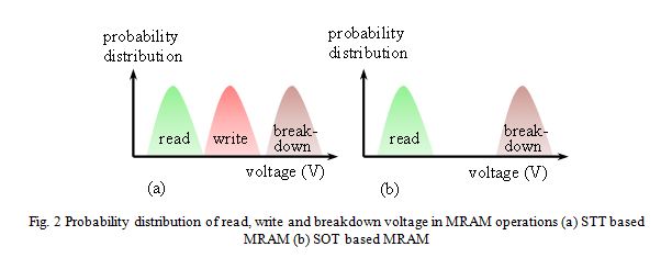
Due to the common write and read path in standard STT switching, we typically have |read voltage| < |write voltage| < |breakdown voltage|. The major issue in MRAM based on STT devices is the interference of these three domains (figure 2(a)) since we have a common read and write path through the junction The process variation at the wafer level as well as the device level mismatches, increase the risk to make the three voltage distributions overlap causing the MRAM failure. Thus, the reliability of STT based MRAMs is dramatically deteriorated. By contrast, figure 2(b) shows that only the interference between the read and breakdown voltages matters for the 3-terminal SOT device, since the writing operation is achieved independently by an in-plane current without passing through the junction. That’s why in figure 2 (b), we do not represent the voltage write domain in the same graph since the write path is independent and does not interfere neither with the read voltage domain nor with the breakdown voltage
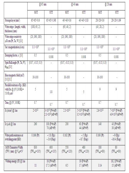
The switching mechanisms of STT and SOT devices have been widely discussed in literature and many macro models have been proposed to describe the behavior of such devices [4][5][7][8][9][10]. In our study, spice-like compact models -developed in Verilog-A language- have been used for each technology. Both STT and SOT compact models are developed according to the same magnetic assumptions in table 1.
3.Evaluation results
A basic key toward MTJs perfection is the materials engineering development and magnetic processes optimization. Increasing the thermal stability, decreasing the switching current, maintaining a solid switching probability and keeping high reliability are the golden rules when scaling MTJ devices.
Many papers investigated sub-100 nm STT-MTJ samples and modeled their behavior to drive predictive studies at an extended scalability [5]. To the best of our knowledge, the smallest feature size of a STT-MTJ ever reported is 17 nm [11]. The sample was fabricated by using perpendicular materials with high interface anisotropy of 2.5 erg/cm² and improved integration processes. The fabricated device achieved reproducible switching with critical current (Ic) of 44 µA at 100 ns writing pulse, tunneling magneto-resistance (TMR) ratio of 70% and thermal stability factor (E/kBT) of 34.
Concerning SOT-MTJs, the concept is much younger than its STT counterpart. At first, it has been reported in 2011 [6]. Since then, it has become a hot topic in both academics and industrials. Samples with a variety of materials combination have been fabricated [12][13][14][15] and physical models have been proposed to understand the behavior of SOT devices [7][8][9][10]. While the MTJ barrier material could be MgO or AlOx, the writing electrode heavy materials existing in literature to fabricate the SOT device are: Tantalum (Ta), Tungsten ![]() or Platinum (Pt). The spin hall (SH) angle and the resistivity are the two main material characteristics which matters for the SOT-MTJ; The SH angle determines the spin injection efficiency of the material. The resistivity of the material plays a fundamental role in the minimization of the writing energy since it determines the resistance of the writing path. The smallest dimension of the SOT device published in literature is a (135 nm × 135 nm) MTJ on top of a writing stripe of 210 nm of length, 135 nm of width and 3 nm of thickness [12]. In [13], it has been shown that the spin hall injection efficiency (ratio of spin current injected to the charge current in the electrode) as a function of electrode thickness has an optimum value at 2-3 nm electrode thickness. Based on all these latter considerations, the geometry ratios of the SOT device are shown in figure 2(c). Concerning the current density to switch the magnetization, both theoretical models and experimental results agree on the fact that a magnitude of ~2×10¹² A/m² is required for fast switching (≤ 1 ns) [7][8][9][10][11][12].
or Platinum (Pt). The spin hall (SH) angle and the resistivity are the two main material characteristics which matters for the SOT-MTJ; The SH angle determines the spin injection efficiency of the material. The resistivity of the material plays a fundamental role in the minimization of the writing energy since it determines the resistance of the writing path. The smallest dimension of the SOT device published in literature is a (135 nm × 135 nm) MTJ on top of a writing stripe of 210 nm of length, 135 nm of width and 3 nm of thickness [12]. In [13], it has been shown that the spin hall injection efficiency (ratio of spin current injected to the charge current in the electrode) as a function of electrode thickness has an optimum value at 2-3 nm electrode thickness. Based on all these latter considerations, the geometry ratios of the SOT device are shown in figure 2(c). Concerning the current density to switch the magnetization, both theoretical models and experimental results agree on the fact that a magnitude of ~2×10¹² A/m² is required for fast switching (≤ 1 ns) [7][8][9][10][11][12].
In our study, we target fast switching applications of NV-MRAM. Thus, the values of critical currents calculated in table 1 correspond to a switching operation of 1ns pulse.
The CMOS design kits used for this study are 65 nm, 40 nm and 28 nm from the same semiconductor foundry. This faithfully corresponds to the dimensions of MTJs we aim to evaluate. All assumptions about the parameters and the electrical performance shown in table 1 correspond closely to results published in literature about the SOT and STT devices.
4.Discussion
The main goal of our study is to investigate the requirements for the writing operation in term of transistor sizing and energy. But, we briefly shed the light on the reading operation. We recall that the STT device is limited by the applied voltage which should not attain the breakdown voltage. Thus, it limits the increase of Resistance Area (RA) and consequently a high error rate of reading circuits. The resistance of the MTJ should be in the same order of that of a CMOS transistor (few KΩ). Low MTJ resistance leads to a high error rate in MRAM applications because the process variation of the CMOS part can cover the resistance of the MTJ and definitely fake the reading phase. In the case of sub-40 nm dimensions, we notice that such an issue is omitted; the resistance of the STT-MTJ (> 5 KΩ) has the same magnitude of CMOS transistors leading to more reliable read operation in memory applications. However, a particular attention should be paid to the reading current to not overlap with the writing current domain and so bring out an undesirable switching. In the case of SOT technology, the write and read paths are independent, so there is no real limitation in terms of RA. It can be freely engineered to correspond to the favorable resistance required by MRAM applications and so increase their robustness.
Concerning the writing operation of MTJs, 1 MTJ is usually associated to a selection transistor to make 1 bit-cell architecture. At a given supply voltage (Vdd), the size and the polarization of the transistor determine the amount of current which flows through the junction. To keep the high density feature of MTJ-based MRAMs, it is not judicious to use a large bit-cell transistor for each MTJ. Table 1 shows that smaller transistors are required for the STT device at both nodes when compared to its SOT counterpart. This is mainly due to the high current density (and consequently the writing current) required to switch SOT-MTJs. At 28 nm dimension, STT-MTJ based circuits could be designed with the minimum transistor size (80 nm transistor width). Such a result opens the doors for ultra-dense MRAMs and eases the integration of STT-MTJ in full digital design flows. Results show that at sub-65 nm scale, the STT device overcomes the SOT device in terms of required transistor size and consequently the overall area. The required area per SOT-based bit-cell would be larger, if we envisage using a bit-cell structure with two transistors instead of one for the 3-terminal structure of the SOT device. In general, results concerning the size of transistors required for both (STT and SOT) MTJs are still very reasonable at sub-65 nm scale, especially when compared with the 6 transistors required for the SRAM bit-cell. With the current state of art, the SOT device does not use the minimum transistor size. In one hand this decreases the bit-cell density, in the other hand the immunity to the CMOS process variation is enhanced since larger transistors are used.
As we explained in section 2, the writing mechanism of the SOT-MTJ is different from its STT counterpart since an in-plane current is applied through the stripe line conductor avoiding the passage through the junction. Thus, the electrical stress on the barrier is relaxed and endurance is improved. Benefits in terms of energy per bit-cell can be also observed; since, the writing stripe is highly conductive (Pt, W, Ta), the writing path has a very low resistance (Rw). If we consider Ic the critical writing current and τ =1ns the width of the writing pulse, the energy per bit-cell can be calculated as (E= Rw × Ic2 × τ). In our study, we consider the case of Platinum (Pt) with low resistivity value (20 µΩ.cm). According to the geometry dimension ratios proposed in figure 2 (c), an improvement of 3× and 6× is observed in favor of the SOT device when compared with the energy required for the STT device at 40 nm and 28 nm dimensions, respectively. This ratio could be diminished if we use other heavy materials such as the Tantalum (Ta) or the Tungsten ![]() which have a resistivity nearly 10× higher than Platinum. Intensive research about the best material trade-off combination in terms of resistivity, SH angle, TMR… is under progress [12][13][14][15].
which have a resistivity nearly 10× higher than Platinum. Intensive research about the best material trade-off combination in terms of resistivity, SH angle, TMR… is under progress [12][13][14][15].
For a given applied voltage, the very low resistance of the write path offers the possibility to attain a high write current. When associated to the semi-processional switching nature of SOT devices [9][10], ultrafast speed can be attained. Experimental results of the SOT device show that it is possible to switch at only 380ps [12]. Theoretical predictive studies of the SOT technology proclaim that the SOT device can perform 4× faster with a decrease of 20× in term of energy [1] when compared with STT-MTJ. Also, a predictive study of an ellipsoidal SOT device with dimensions of (30 nm × 60 nm) claims that at low voltage, an improvement of more than 100× can be achieved in term of energy-delay [13].
It is worth noticing that the SOT technology has a symmetrical writing current. Almost, the same current is required to switch from parallel to antiparallel state and vice-versa. As shown in table 1, this is not the case for the STT device where a greater current is required to switch from parallel to antiparallel state.
Finally, it is worth noticing that in our study, we did not consider the process variation and devices mismatches. At very advanced nodes, both (CMOS and magnetic) processes suffer from a lack of maturity leading to a considerable process variations at the wafer level. Thus, the achievement of reliable and dense MRAMs is still related to the progress of materials engineering and the development of processes tools. At the design level, the proposal of robust MRAM architectures can alleviate some technological locks.
5.Conclusion
The Advanced technology nodes VLSIs suffer from high leakage current. The concept of “hybrid CMOS” integrated circuits (ICs) could be an efficient remedy for such a dilemma. The integration of non-volatile memories, such as MRAMs, closer to the logic reduces the power consumption and increases the bandwidth between memory and logic. In this study, simulation results with MTJ dimensions of 65 nm, 40 nm and 28 nm for STT and SOT switching devices showed that a transistor size (width) of 400 nm to 550 nm is required with 40 nm technology. The minimum size of transistor (80 nm width) can be used in the case of STT-MTJ based bit-cell with 28 nm technology node. The reasonable size of required transistors by bit-cell confirms the density criteria of MTJ based MRAMs at scaled dimensions. The SOT device overcomes its STT counterpart in term of writing energy by a factor of 3× and 6× at 40 nm and 28 nm dimensions, respectively. While it is still in its infancy, the SOT switching needs high current density leading to a high critical current. However, researchers are optimistic about the future of the SOT-MTJ and envisage engineering techniques which could decrease the switching current in order to be competitive with the current STT state of the art.
6.Acknowledgments
This project has received funding from the European Union’s Horizon 2020 research and innovation program under grant agreement n°687973.
7.References
[1] K. Jabeur, Fabrice Bernard-Granger, G. Di Pendina, G. Prenat, ‘Spin Orbit Torque Non-Volatile Flip-Flop for High Speed and Low Energy Applications’, IEEE electron device letters, vol. 35, no. 3, march (2014)
[2] Everspin (2012). [Online] Available: http://www.everspin.com
[3] L. Prejbeanu, M. Kerekes, R. C. Sousa, H. Sibuet, O. Redon, B. Dieny, and J. P. Nozieres, “Thermally assisted MRAM”, J. Phys, -Condens. Matter, p. 165218, (2007)
[4] Kang,W., Zhao,W., Klein,J-O., Wang,Z., Y,Zhang., Zhang,Y.,Ravelosona, D.,Chappert,C., ‘An Overview of Spin-based Integrated Circuits, Proceedings of IEEE ASP-DAC, (2014)
[5] Ki Chul Chun, Hui Zhao, Jonathan D. Harms, Tae-Hyoung Kim, Jian-Ping Wang and Chris H. Kim,’ A Scaling Roadmap and Performance Evaluation of In-Plane and Perpendicular MTJ Based STT-MRAMs for High-Density Cache Memory’, IEEE journal of solid-state circuits, vol. 48, no. 2, February (2013)
[6] Miron, I.M., Garello,K., Gaudin,G., Zermatten, P-J.,Costache, M-V., Auffret, S., Bandiera, S. Rodmacq, B., Schhuhl, A., Gambardella, P., (2011), ‘Perpendicular switching of a single ferromagnetic layer induced by in-plane current injection’, Nature 476, (2011)
[7] K. Jabeur, G. Prenat, G. Di Pendina, L. D. Buda Prejbeanu, I. L. Prejbeanu, B. Dieny, ‘Compact model of a three-terminal MRAM device based on Spin Orbit Torque switching’, ISCDG Proceedings, (2013)
[8] K. Jabeur, L. Buda-Prejbeanu, G. Prenat, G. Pendina, ‘Study of Two Writing Schemes for a Magnetic Tunnel Junction Based On Spin Orbit Torque’, World Academy of Science, Engineering and Technology, International Science Index 80, International Journal of Electrical, Electronic Science and Engineering, 7(8), 497 – 503 (2013)
[9] Ki-Seung Lee, Seo-Won Lee, Byoung-Chul Min, Kyung-Jin Lee, ‘Thermally activated switching of perpendicular magnet by spin-orbit spin torque’, arXiv:1401.2266 [cond-mat.mtrl-sci], (2014)
[10] Ki-Seung Lee, Seo-Won Lee, Byoung-Chul Min and Kyung-Jin Lee, “Threshold current for switching of a perpendicular magnetic layer induced by spin Hall effect”, Appl. Phys. Lett. 102, 112410 (2013)
[11] Woojin Kim, J. H. Jeong, Y. Kim, W. C. Lim, J. H. Kim, J. H. Park, H. J. Shin, Y. S. Park, K. S. Kim, S. H. Park, Y. J. Lee, K. W. Kim, H. J. Kwon, H. L. Park, H. S. Ahn, S. C. Oh, J. E. Lee, S. O. Park, S. Choi, H. K. Kang, C. Chung, ‘Extended scalability of perpendicular STT-MRAM towards sub-20nm MTJ node ‘, pp (531-534), IEDM (2011)
[12] K. Garello, C. O. Avci, I. M. Miron, O. Boulle, S. Auffret, P. Gambardella, G. Gaudin,’ Ultrafast magnetization switching by spin-orbit torques‘, arXiv:1310.5586v1 (2013)
[13] S. Manipatruni, D.E. Nikonov, I.A. Young, ”Voltage and Energy-Delay Performance of Giant Spin Hall Effect Switching for Magnetic Memory and Logic”, Cornell Univ. Press, pp1-16 (2013)
[14] L. Liu et al. “Spin-Torque Switching with the Giant Spin Hall Effect of Tantalum”, Science 336, 555, (2012)
[15] J. Guo et al, “MRAM Device Incorporating Single-Layer Switching via Rashba-Induced Spin Torque”, IEEE transactions on magnetics, vol. 47, no. 10, October (2011)
Authors
Kotb Jabeur received the PhD degree in September 2012 from Ecole Centrale de Lyon, France. Then, he held a 2-years postdoctoral researcher position at SPINTEC (CEA/CNRS/INAC) involved in modelling and design with spintronic devices. Since 2015, he worked as memory design engineer at EVADERIS. Now, he is a research scientist at SPINTEC (CEA/CNRS/INAC). His research activities and interests mainly include compact modeling of emerging nano-devices and memory design. He has over 7 years’ experience in microelectronics with reserach labs and industrials.
 Gregory Di Pendina received the master’s degree in 2005 from the Joseph Fourier University, Grenoble, France, and the PhD degree in 2012 from the University of Grenoble, France. He has been an engineer-researcher at CNRS (National Scientific Research Center) for 17 years. His research interest is MRAM-based non-volatile analog and digital design mainly for ultra-low power applications such as Internet of Things (IoT) and harsh environment such as space applications.
 Guillaume Prenat graduated from Grenoble Institute of Technology in France, in 2002. He received the PhD degree in the field of analog and mixed signal testing in 2005. He is a researcher in microelectronics now in charge of the design activity for the CEA-SPINTEC Lab. He joined the spintronics laboratory SPINTEC as a CEA researcher in November 2006 to take in charge the design activity. His field of interest covers the development of design tools for the hybrid CMOS/magnetic technology and the evaluation of hybrid nonvolatile circuits (FPGA, processors…) to contribute to circumvent the limits of microelectronics. He holds 6 several international patents and has authored or co-authored more than 40 international scientific publications in this field.
